
 020-84858360
020-84858360
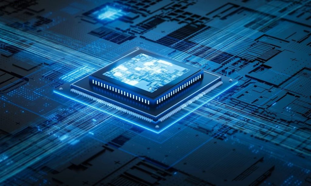
At TSMC’s 3nm production line, a mere 0.5-micron particle can destroy wafers worth millions. SEMI data reveals that global semiconductor fabs suffer $5 billion+ annual losses due to yield gaps from cleaning processes—a stark testament to nanoscale manufacturing’s zero-tolerance for contamination.
AOQUN’s Engineering R&D Center, backed by 20 years of expertise and partnerships with Sun Yat-sen University, Jinan University, and others, has pioneered the Intelligent Damage-Free Pcb Cleaning Brush (Patent: ZL202411907351). This "nano vacuum"-like solution empowers the semiconductor industry to shatter cleaning barriers.
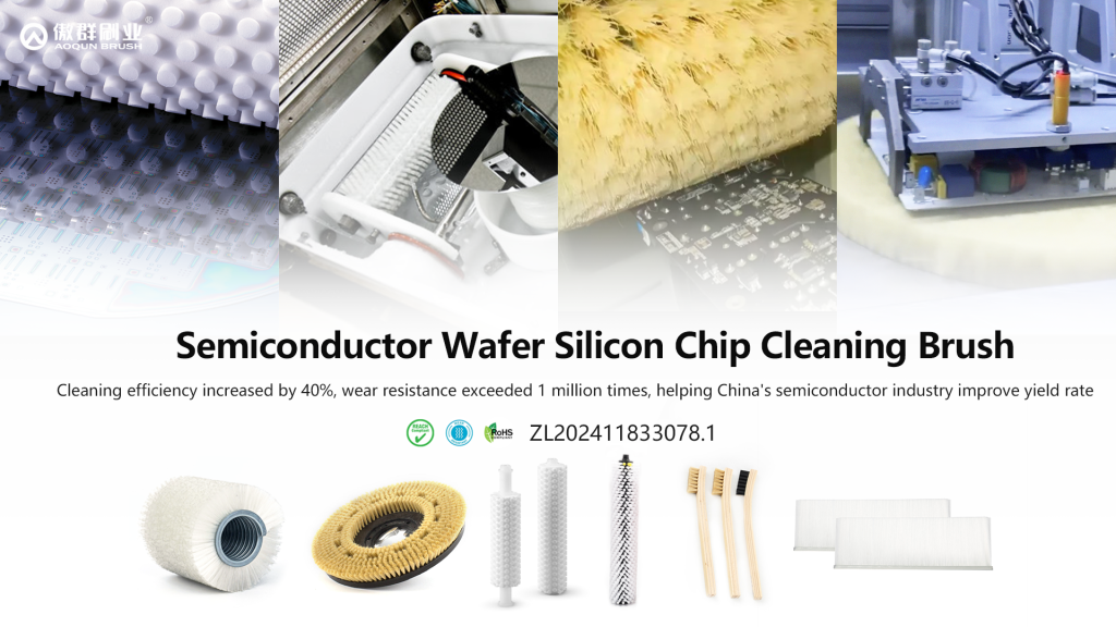
▶ Zero-Damage Precision
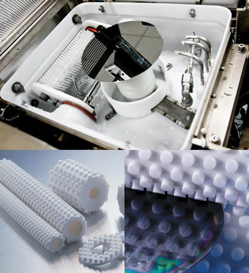
Withstands 1 million+ friction cycles via ultra-elastic, wear-resistant design.Exceptional flexibility removes contaminants without scratching wafer surfaces.
▶ Revolutionary Contaminant Removal
Eliminates stubborn residues (CMP slurry, metal debris) through directional fiber alignment technology, ensuring uniform pressure distribution. This achieves:
✓ 40% higher cleaning efficiency
✓ Zero surface damage
✓ Replaces German/EU/Japanese polishing tools
AOQUN’s Chip cleaning solutions span:
With 250 million annual capacity, AOQUN meets high-volume, high-precision demands of global semiconductor leaders.
AOQUN will advance material science and digital production to tackle cleaning challenges in sub-nm processes and high-frequency applications—empowering the IoT era with micron-perfect purity.


scan to wechat

scan to wechat


